

ShenZhen CityYong jation Technology Co., Ltd
Tel:0755- 23726506
0755- 23014364
E-mail:sz@yjxunpcb.com
Web:www.yjxunpcb.com
Shenzhen project address:Building 13th ,Sha Er bluesky technology park ,Shajing .Baoan ,ShenZhen City,GuangDong .China .
Jiangxi Factory Address:Building D, Yunling Industrial Zone, Suichuan County, Ji'an City, Jiangxi Province, China
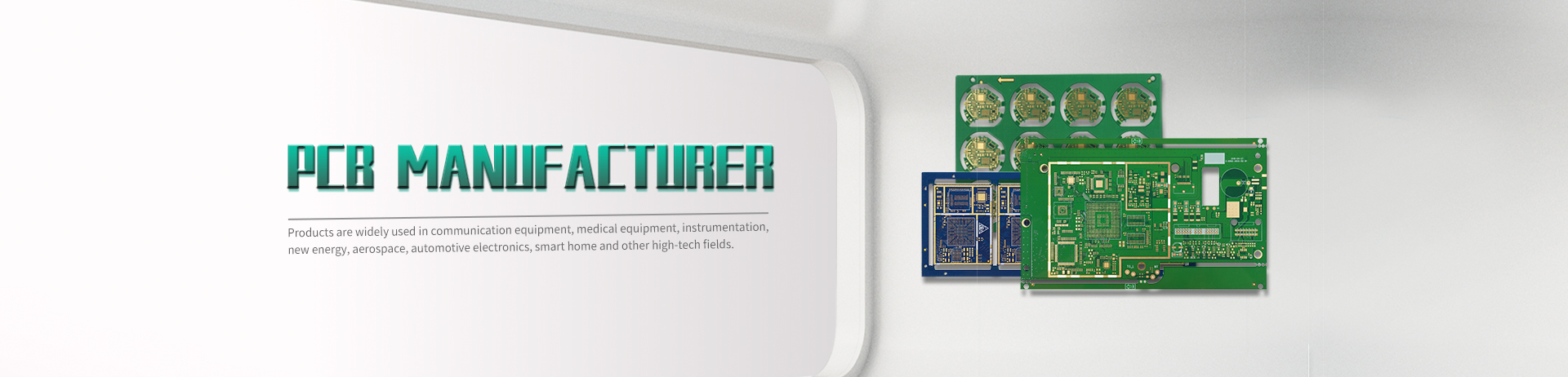
PCB (Printed Circuit Board) printed board, also called printed circuit board, printed circuit board. A multi-layer printed board refers to a printed board with more than two layers. It is composed of connecting wires on several layers of insulating substrates and pads for assembling and soldering electronic components. The role of insulation.
PCB multi-layer board refers to the multi-layer circuit board used in electrical products, and the multi-layer board uses more single-sided or double-sided wiring boards. A printed circuit board with a double-sided inner layer, two single-sided outer layers, or two double-sided inner layers and two single-sided outer layers, alternated together by a positioning system and insulating bonding materials, and conductive patterns. Printed circuit boards that are interconnected according to design requirements become four-layer and six-layer printed circuit boards, also known as multi-layer printed circuit boards.
With the continuous development of SMT (Surface Mount Technology) and the continuous introduction of a new generation of SMD (Surface Mount Devices), such as QFP, QFN, CSP, BGA (especially MBGA), electronic products are made more intelligent and miniaturized, so It has promoted the major reform and progress of PCB industry technology. Since IBM first successfully developed a high-density multilayer board (SLC) in 1991, major groups in various countries have also successively developed a variety of high-density interconnect (HDI) microplates. The rapid development of these processing technologies has prompted the PCB design to gradually develop in the direction of multi-layer and high-density wiring. Multilayer printed boards have been widely used in the production of electronic products due to their flexible design, stable and reliable electrical performance and superior economic performance.
Current Situation and Development of Multilayer Printed Boards
Since the middle and late 1980s, the output value and output of multi-layer boards have increased by more than 10% (compared with the previous year) every year. Due to the rapid development of components to be "light, thin, short and small" Multilayer boards will surely become the most influential and vital category in the printed circuit board industry, and become the leading product. Development. Multi-layer boards require higher investment in equipment and technology. In the future, high-level multi-layer boards will be developed and produced in powerful PCB manufacturers
PCB multilayer board features
The biggest difference between PCB multilayer boards and single-sided and double-sided boards is that the internal power layer (maintaining the internal electrical layer) and the ground layer are added. The power and ground networks are mainly routed on the power layer. However, the multi-layer board wiring is mainly based on the top layer and the bottom layer, supplemented by the middle wiring layer. Therefore, the design of the multi-layer board is basically the same as the design method of the double-sided board. The key lies in how to optimize the wiring of the inner electrical layer, so that the wiring of the circuit board is more reasonable and the electromagnetic compatibility is better.
Product
HDI PCB Rigid-flex board High Multilayer PCB Special PCB board High frequency high speed PCB Semiconductor test boardContact
contact us
Copyright © ShenZhen CityYong jation Technology Co., Ltd. 备案号:粤ICP备2021171504号