

ShenZhen CityYong jation Technology Co., Ltd
Tel:0755- 23726506
0755- 23014364
E-mail:sz@yjxunpcb.com
Web:www.yjxunpcb.com
Shenzhen project address:Building 13th ,Sha Er bluesky technology park ,Shajing .Baoan ,ShenZhen City,GuangDong .China .
Jiangxi Factory Address:Building D, Yunling Industrial Zone, Suichuan County, Ji'an City, Jiangxi Province, China
negative film of pcb circuit board
Generally speaking, the solution used in the negative film process is an acid-base corrosion process. After the film is formed, the desired channel or copper surface is completely transparent, and the undesired part is black. After the route process is exposed, because the dry film inhibitor is exposed to sunlight, the completely transparent part will be chemically hardened, and the following development process will not make the film hard, and the dry film will be washed away, so in the etching process, Only the dry film washed away part of the copper deposition (black part of the negative), and the preserved dry film was not washed away, which is what we want for the pcb board (clear part of the negative).
Positive film of pcb circuit board
Generally speaking, the positive film process is based on the alkaline etching process. On the negative, the desired channel or copper surface is black, and the undesired part is completely transparent. Similarly, after the route process exposure, the completely clear part is hardened by the chemical action of the dry film blocker exposed to the sun, the subsequent development process will wash away the dry film without the hard substrate in the next process, we use alkali The copper surface without tin and lead protection (the transparent part of the negative film) is cut off by the sexual solution, and the part of the pcb circuit board (black film) is left.
The difference between the positive film and the negative film of the pcb circuit board
① Distinguish screen printing screen (negative film), working film, positive film, negative film and film surface: screen printing screen has mother film and working film (sub film), black and yellow film, positive film and negative film;
②The negative film is also called black film, also known as carbon negative film. However, job negatives are not only yellow films, but also black films to make workpieces. It is mainly used to make high-precision HDI boards or save costs, and it is used for one-time mass production and pcb circuit board production in small batch production and production of pcb circuit boards.
③ When the surface of the film is different, the bright side of the black film is the film, while the yellow film is the opposite. Generally speaking, it can be seen that the side is based on the film surface of the graffiti pen or knife head on the screen printing.
④ Precautions for the use of yellow film: There are two types of surface: lubricated and matte, and the second type of application simply shows oil surface indentation.
⑤ The negative film (containing copper) that transmits light on the film circuit is the positive film; the positive film is used in the pattern electroplating process, the developer is dripped as the way, and the remaining function is the corrosion-resistant electroplating process, and the key inlays are lead and tin. Thin films are usually used in the instant etching process, the corrosion resistance after the developer is the way, and the acid-base etching solution is used for the instant etching process.
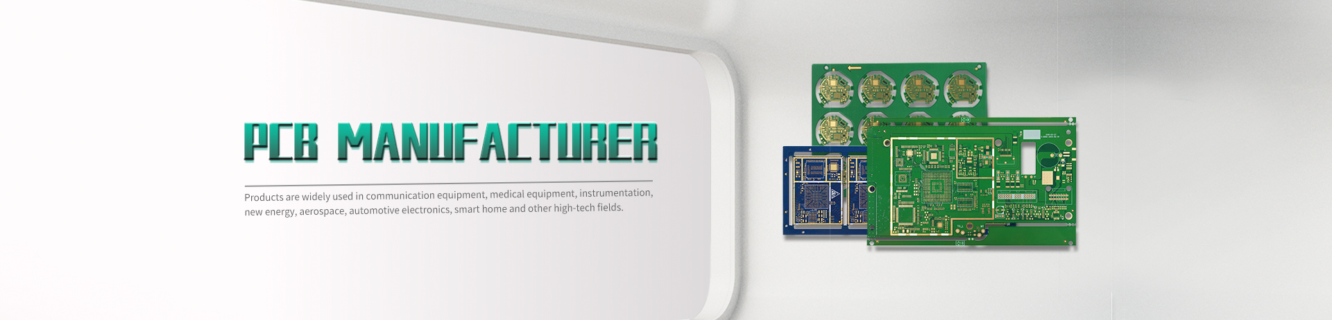
Product
HDI PCB Rigid-flex board High Multilayer PCB Special PCB board High frequency high speed PCB Semiconductor test boardContact
contact us
Copyright © ShenZhen CityYong jation Technology Co., Ltd. 备案号:粤ICP备2021171504号