

ShenZhen CityYong jation Technology Co., Ltd
Tel:0755- 23726506
0755- 23014364
E-mail:sz@yjxunpcb.com
Web:www.yjxunpcb.com
Shenzhen project address:Building 13th ,Sha Er bluesky technology park ,Shajing .Baoan ,ShenZhen City,GuangDong .China .
Jiangxi Factory Address:Building D, Yunling Industrial Zone, Suichuan County, Ji'an City, Jiangxi Province, China
Electronic products are constantly developing towards high density and high precision. The so-called "high" not only improves the function of the machine, but also reduces the size of the machine. High Density Integration (HDI) technology can enable further miniaturization of end product designs while meeting higher specifications for electronic functionality and power. At present, many popular electronic products, such as mobile phones, digital cameras, notebook computers, car electronics, etc., use HDI boards. With the upgrading of electronic products and the needs of shopping malls, the development of HDI boards will be very rapid.
What is an HDI board?
HDI board (High Density Interconnector), that is, a high-density interconnect board, is a circuit board with a relatively high line distribution density using the technology of micro-blind and buried vias. The HDI board has inner layer lines and outer layer lines, and then uses drilling, in-hole metallization and other processes to complete the internal connection of each layer of lines.
HDI board is generally made by lamination method, the more times the lamination is, the higher the skill level of the board. Ordinary HDI boards are basically layered once, and high-end HDIs use two or more layer-up technologies, together with advanced PCB technologies such as stacking, electroplating, and laser direct drilling. When the density of the PCB is increased to more than eight layers, it is made with HDI, and the cost will be lower than the traditional and complex lamination process.

The electrical function and signal correctness of HDI boards are higher than traditional PCBs. In addition, HDI boards have better improvements in terms of radio frequency interference, electromagnetic wave interference, electrostatic discharge, heat conduction, etc. High Density Integration (HDI) technology can enable further miniaturization of end product designs while meeting higher specifications for electronic functionality and power.
The HDI board uses blind hole electroplating and then performs secondary pressing, which is divided into first-order, second-order, third-order, fourth-order, and fifth-order. The first order is relatively simple, and the process and technology are easy to control. The first problem of the second order is the alignment problem, and the second is the problem of punching and copper plating. There are many kinds of second-order designs. One is that each order is staggered. When it is necessary to connect the sub-adjacent layer, it is connected to the middle layer through wires. The method is equivalent to two first-order HDIs. The second is that the two first-order holes are overlapped, and the second-order is completed by the superposition method. The processing is similar to the two first-order holes, but there are many process points that need to be specially controlled, which is mentioned above. The third is to punch holes directly from the outer layer to the third layer (or N-2 layer). The second-order analogy is about the third-order.
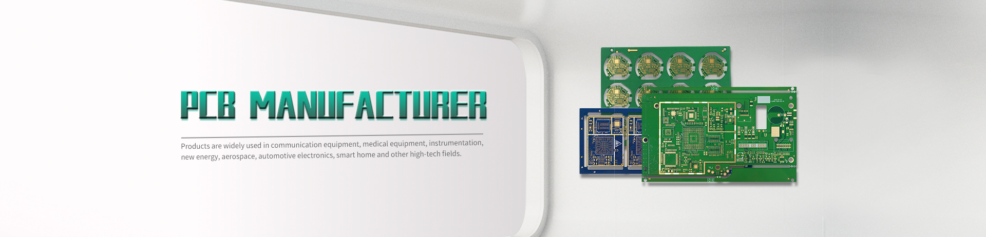
PCB, the Chinese name is printed circuit board, also known as printed circuit board, is an important electronic component, a support body for electronic components, and a carrier for electrical connection of electronic components. The common PCB board is mainly FR-4, which is made of epoxy resin and electronic-grade glass cloth.
Product
HDI PCB Rigid-flex board High Multilayer PCB Special PCB board High frequency high speed PCB Semiconductor test boardContact
contact us
Copyright © ShenZhen CityYong jation Technology Co., Ltd. 备案号:粤ICP备2021171504号