

ShenZhen CityYong jation Technology Co., Ltd
Tel:0755- 23726506
0755- 23014364
E-mail:sz@yjxunpcb.com
Web:www.yjxunpcb.com
Shenzhen project address:Building 13th ,Sha Er bluesky technology park ,Shajing .Baoan ,ShenZhen City,GuangDong .China .
Jiangxi Factory Address:Building D, Yunling Industrial Zone, Suichuan County, Ji'an City, Jiangxi Province, China
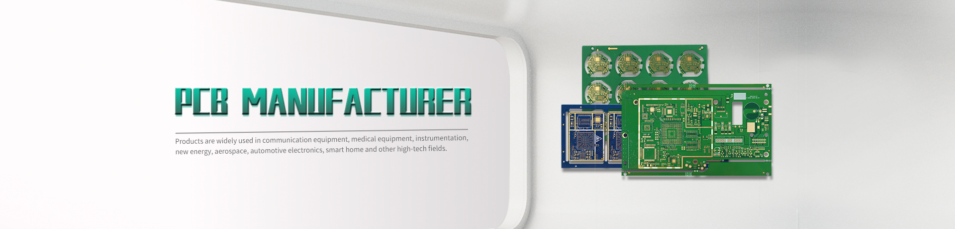
HDI circuit board is the English abbreviation of High Density Interconnector. High Density Interconnection (HDI) manufacturing is one of the fastest growing areas in the printed circuit board industry.
HDI is the English abbreviation of High Density Interconnector, and high-density interconnect (HDI) manufacturing is one of the fastest growing areas in the printed circuit board industry. From HP's first 32-bit computer in 1985, to today's large client servers with 36 sequentially laminated multi-layer printed boards and stacked micro-vias, HDI/micro-via technology is undoubtedly the PCB architecture of the future. Larger ASICs and FPGAs with smaller device pitches, more I/O pins, and embedded passives have increasingly shorter rise times and higher frequencies, all of which require smaller PCB feature sizes, driving demand for Strong demand for HDI/micro vias. HDI process
HDI imaging
1. While achieving low defect rate and high output, it can achieve stable production of HDI's conventional high-precision operation.
E.g:
*Advanced mobile phone board, CSP pitch less than 0.5mm (connection [with or without wires between boards]
*The board structure is 3+n+3, with three stacked vias on each side, *6 to 8-layer ironless printed boards with stacked vias
In terms of imaging, such designs require ring widths less than 75µm, and in some cases even less than 50µm. These inevitably lead to low yields due to alignment issues. Additionally, driven by miniaturization, lines and pitches are getting finer—meeting this challenge requires a change in traditional imaging methods. This can be done by reducing the panel size, or by imaging the panel in several steps (four or six) using a shutter exposure machine. Both methods achieve better alignment by reducing the effects of material deformation. Changing the panel size resulted in a high cost of materials, and the use of a shutter exposure machine resulted in low throughput per day. Neither method can fully address material deformation and reduce plate-related defects, including the actual deformation of the plate as the batch/lot is printed.
2. Achieve the required output by printing the required number of panels per day. As previously mentioned, the relative quantities of yields required should be factored into the accuracy requirements. To achieve the required output, it is necessary to obtain a high output rate with the help of automatic control.
3. Low cost operation. This is a major requirement for any volume manufacturer. In the early LDI mode, it was required to replace the traditionally used dry film with a more sensitive dry film to achieve faster imaging speed; or according to the light source used in the LDI mode, the dry film was replaced with a different wavelength band. In all of these cases, the new dry film will usually be more expensive than the traditional dry film used by the manufacturer.
4. Compatible with existing processes and production methods. Processes and methods of mass production are usually carefully specified to meet the requirements of mass production. The introduction of any new imaging method should have minimal changes to existing methods. This includes minimal variation in the dry film used, the ability to expose individual layers of solder mask, traceability capabilities required for mass production, and more.
Product
HDI PCB Rigid-flex board High Multilayer PCB Special PCB board High frequency high speed PCB Semiconductor test boardContact
contact us
Copyright © ShenZhen CityYong jation Technology Co., Ltd. 备案号:粤ICP备2021171504号