

ShenZhen CityYong jation Technology Co., Ltd
Tel:0755- 23726506
0755- 23014364
E-mail:sz@yjxunpcb.com
Web:www.yjxunpcb.com
Shenzhen project address:Building 13th ,Sha Er bluesky technology park ,Shajing .Baoan ,ShenZhen City,GuangDong .China .
Jiangxi Factory Address:Building D, Yunling Industrial Zone, Suichuan County, Ji'an City, Jiangxi Province, China
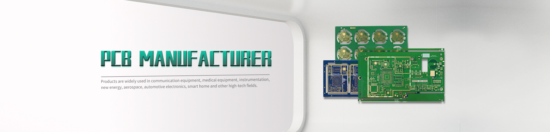
Regarding the printed circuit board, I believe that electronic workers are not unfamiliar, it is an indispensable part of modern electronics. How much do you know about its production process? Let's find out.
The substrate of the printed circuit board itself is made of insulating and non-bending materials, and the small circuit material visible on the surface is copper foil. During the manufacture of the circuit board, the remainder of the circuit board is etched into a small section.
These circuits are called wires or wires, and are used to supply circuit connections between components on a circuit board. Generally, the color of the printed circuit board is green, which is the color of the solder mask, which is an insulating protective layer that can protect the copper wire to prevent the parts from being soldered to the wrong place.
The manufacturing process of a printed circuit board begins with a PCB "substrate" made of glass epoxy or similar material. The first step in fabrication is to draw the lines between the parts. The method is to "print" the negative electrode of the printed circuit board on the metal conductor by means of negative migration.
A layer of copper foil can eliminate the remaining layer. For double-sided production, both sides must be covered with copper foil, and to make a multi-layer board, two double-sided boards can be pressed together with a special adhesive.
Next, we were able to drill and plate the components on the printed circuit board. After the mechanical equipment is drilled according to the drilling requirements, it is necessary to use plated through hole technology (PTH) for the lining of the hole wall. Make sure that the inner wires of each layer of in-hole metallization can meet each other.
Before electroplating, it is necessary to remove impurities in the holes. This is due to the fact that the epoxy undergoes some chemical changes when heated, it masks the inner layers of the PCB, so it should be removed first. Both cleaning and plating operations are performed in a chemical process. Next, you need to cover the outer wires with solder mask so that the wires don't touch the plated parts.
Then, the symbol screen of each component is printed on the circuit board to symbolize the orientation of each component. Do not cover any wires or gold fingers, as it will reduce the stability or solderability of the current connection. In addition, if there is a metal connection, the position of the gold finger needs to be gold-plated, which can ensure high-quality connection current when inserted into the expansion slot.
Then comes the quiz. To test whether a printed circuit board is shorted or open, optoelectronic testing can be used. Optical scanning is used to detect defects on each layer, while electronic testing generally uses a flying probe to check all connections. Electronic tests are more accurate for shorts or opens, but optical tests are easier to detect incorrect gaps in conductors.
Product
HDI PCB Rigid-flex board High Multilayer PCB Special PCB board High frequency high speed PCB Semiconductor test boardContact
contact us
Copyright © ShenZhen CityYong jation Technology Co., Ltd. 备案号:粤ICP备2021171504号